Характеристики
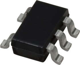
SN74LVC1G125DBVR, Один буферный элемент с тремя состояниями …The SN74LVC1G125DBVR is a Bus Buffer Gate IC, designed for 1.65 to 5.5V VCC operation. This device is a single line driver with a 3-state output. The output is disabled when the output-enable (OE) input is high. The CMOS device has high output drive while maintaining low static power dissipation over a broad VCC operating range.
• Supports 5V VCC Operation
• Input Accepts Voltage to 5.5V
• Provides Down Translation to VCC
• 3.7ns at 3.3V Maximum Propagation Delay Time
• Low-power Consumption, 10µA Maximum ICC
• ±24mA Output Drive at 3.3V
• Ioff Supports Live Insertion, Partial-power-down Mode and Back-drive Protection
• Latch-up Performance Exceeds 100mA Per JESD 78, Class II
• Green Product, No Sb/Br
 Личный кабинет


 Загрузка